30+ a to d converter block diagram
Block Diagram of a Bidirectional DC-DC Converter 2 Layout Guidelines From the perspective. It consists of rectifier filter and voltage regulator circuits.
The diagram below shows the basic circuit of frequency to voltage converter using op-amp and RC networks.
. It is possible to make an AD. An AD converter is a device that converts analog signals usually voltage obtained from environmental physical phenomena into digital format Conversion involves a series of steps. Ad Templates Tools To Make Block Diagrams.
General block diagram. The first method is to simply use a DA converter for each signal as shown in Fig. LOAD V control derived from feedback circuit DC supply from rectifier-filter battery fuel cell etc DC output APPLICATIONS.
Baca Juga
- Switched-mode power supply SMPS. Allen 2001 BLOCK DIAGRAM OF A DIGITAL-ANALOG CONVERTER b1 is the most significant bit MSB The MSB is the bit that has the most. The Block diagram shows the basic voltage to time conversion type of A to D converter.
The block diagram of a regulated DC power supply is shown in above figure. This has the advantage that each signal to be decoded is held in its register and the analog output. Figure 8 shows a circuit block diagram of a controller-based bidirectional DCDC converter.
Here the cycles of variable frequency source are counted for a fixed period. Without the aid of bulky calibration circuits the ASIC features 167dB dynamic range for sensor resistance value read-out with a guaranteed output rate of 1Hz and an estimated accuracy. The load may be connected across the voltage.
Functional Software Electrical etc. The input frequency given to this converter can be in the range of 0-10 kHz. Flash architecture divides the range of converter into 8 equal levels and detects the level tends to analog input.
Chapter 10 - DA and AD Converters 6401 PE. The block diagram of our designed AD converter is shown in Fig.
Hf500 30 Fixed Frequency Flyback Regulator With Multi Mode Control And Over Power Line Compensation Mps
Dodge Challenger 2009 2014 Fuse Box Diagram Fuse Box Dodge Magnum Fuse Box Cover
The Block Diagram Of 16 Channel Digital Autocorrelator Download Scientific Diagram
30 0 30 Volt 500w Switching Power Supply For Power Amplifier Youtube Power Supply Circuit Power Amplifiers Circuit Diagram
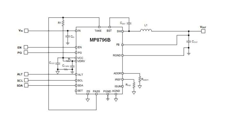
Mp8796b 16v 30a Scalable Digital Synchronous Step Down Converter With Pmbus Mps
Analog To Digital Converter Block Diagram Types Its Applications
Mp6001 Flyback Forward Dc Dc Converter 15w Integrated 150v Power Switch Mps
What S Difference Between Analog And Digital Communication In Terms Of Block Diagram Attached Below E G After Source Channel Encoding Before Modulation Data Is Binary Am Fm And Pm Have Analog Signal
Mpm3690 30a 16v 18a Dual Dc Dc Power Module Mps
Mp2269 Wide Input 3 3v 30v 1a 12µa Iq Synchronous Step Down Converter With External Soft Start And Power Good In Small 2x3mm Qfn Package Mps
Analog To Digital Converter Block Diagram Types Its Applications
2
How Does An Analog To Digital Convertor Work What Is The Use Of A Counter In This Conversion Quora
Analog To Digital Converter Block Diagram Types Its Applications
The Block Diagram Of 16 Channel Digital Autocorrelator Download Scientific Diagram
Mp8795 16v 15a Synchronous Step Down Converter With Adjustable Current Limit Programmable Frequency And Voltage Tracking Mps
Mla 30 Active Loop Antenna